Expect roughly 10 dB per stage 3 STAGE DESIGN. Let me try to find it.
Microwaves101 Distributed Amplifiers
The figure depicts discrete amplifier MMICs used in the design.

. I do have design examples using ADS. W w w ww. 12 where xdxd xd ds ds d C R CR 1 1 w w Using 9-12 the image impedance and propagation factor can be calculated using 4 and 5.
To employ the distributed amplification technique for the design of ultra-wide-band low-noise amplifiers the poor noise performance of the conventional distributed amplifiers DAs needs to. Consequently the focus of this thesis is upon the application of distributed integrated circuit methodologies towards the realization of a distributed broadband amplifier in a commercial CMOS process technology. Expect saturated power to be 35 dBm Input power.
For example as shown in Figure 2 the CMD192C5 distributed amplifier has a positive gain slope with respect to frequency from DC-20 GHz. 1 2 2 2 2 Line losses per section. Selecting an appropriate op amp is an important part in designing an instrumentation amplifier.
In that year Percival proposed a design by which the transconductances of individual vacuum tubes could be added linearly without lumping their element capacitances at the input and output thus arriving at a circuit that achieved a gain-bandwidth product greater than that. I have done it for few years. AMPLIFIERS INTRODUCTION Amplifiers are used extensively in electronic circuits to make an electronic signal bigger without affecting it in any other way.
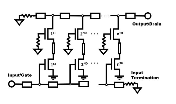
Figure B1 shows the result of equalizing the lines to Cds and Figure B2 shows the result of equalizing the lines to Cgs. The name distributed amplifier first introduced in Ginzton 48. Input output and intermediate.
The signal source also determines what kind of signal the DAS distributes. Index Terms - Distributed Amplifier CRLH Transmission Line Diplexer Dual-Band Power Amplifier Power Combiner. It is an extension of the original Distributed Amplifier example to now include Parametric Layout.
Real-World Design Example GSM 900 MHz GaAs HBT PA Design P OUT 33 dBm linear 2 W V CC 35V R LOAD V CC 2 2P OUT 3 Ω I MAX 2V CC R LOAD 233 A Note. No matter how well the distribution system performs a DAS is always limited by the performance of the signal supplying the network. A four section distributed amplifier was designed with the above relations for the two extreme cases.
A distributed amp is a clever way to provide enormous bandwidths as much as 100 GHz. Constant-envelope 5 dBm Gain P OUT P IN 27 dB. Such performance offers considerable advantages to a wideband system designer by eliminating some of these equalization stages and reducing the size power and complexity of the design implementation.
In this two-section example the re ection and transmission coe cient are given by ˆ1 Z02 Z0 Z02 Z0 1 3 1 2Z0 Z02 Z0 4 3 Note that if the currents are properly delayed the reverse currents can cancel J. Input degernation with distributed amplifier at the upper 3 - dB design frequency of the amplifier Suppose we apply degeneration to make G 11new G 22new max 11 22 2 2111 22 221 2 0 221 2 2 max 21 max 11 0 max 22 0 max in 11 0 out 22 0 11 0 4 4 4 Circuit power gain 1 Maximum sections. However with circuit size in mind this design will use the LM324.
Researchers have since managed to design distributed amplifiers with bandwidths exceeding 100 GHz in modern RFIC technologies. The key idea is to absorb parasitic capacitances of the transistors into T-lines to improve the amplifier bandwidth. The CMD304 for example is a DC-67 GHz distributed amplifier with a flat gain response with respect to frequency as shown in Figure 3.
The use of Composite RightLeft-Handed Transmission Lines CRLH-TLs in the design of Distributed Amplifiers DAs has shown the. Radike samantha beng hons nus a thesis submitted for the degree of master of engineering department of electrical and computer engineering national. Some distributed amplifiers can operate down to DC as well so they are used as opto-electronic amps.
Hashemi A 013 m CMOS power ampli er with ultra-wide instantaneous bandwidth for. G G G Y. Load-Line Analysis in the Frequency Domain with Distributed Amplifier Design Examples Abstract.
Examples at X- C- and S-band operation. Almost any op amp will work for this design. The greater bandwidth of figure B1 is apparent about 50 GHz however the design does not achieve any amplification.
An amplifier electronic amplifier or. The three main signal sources are off-air BTSNodeBeNodeB and small cell. There are three stages in the design of SSPA as shown viz.
The plots are generated. Distributed amplifier basic idea first introduced in 1936 Percival 36 to overcome traditional GBW limit of vacuum tube amplifiers. I dont know this approach will be good up to 10 GHz or not.
The LM324 IC has four op amps on the chip. The instrumentation amplifier will require three op amps. The design of the distributed amplifiers was first formulated by William S.
Faculties and often novel design capabilities for a given IC process. These expressions are plotted in figures 6 7 and 8. In Virdees book they use a chip FET and use wire bound as inductors.
Time-Domain analysis of a multi-FET circuit over a wide frequency range and for several power levels using SPICE is not practical because of excessive computer time causing high cost and slow feedback to the designer. Example Solid State RF Power Amplifier Design. Following figure mentions devices used in 5 Watt Low cost Feed Mount Solid State Power Amplifier SSPA for C band application.
Distributed Amplifier This example demonstrates a MMIC design of a distributed amplifier with a flat gain of about 12dB from about 2GHz to 10GHz. Distributed amplifier tutorial I have tried to design some distributed amplifier using the book by Virdee. S-parameters and noise figure versus frequency for the CMD192C5 distributed amplifier.
Example of a 100W Class D Amplifier ENABLE 6 V 6 V 20 V 20 V 47 Ω 10 µF R8 C11 Optional switching noise filter Demodulation LPF Startup resister High-side OCP Bootstrap floating supply charging path Low-side OCP Dead-time Feedback resistor 2nd order integrator Input resistor VAA supply VSS supply DC blocking capacitor Bootstrap floating supply capacitor. Design of a broad-band distributed amplifier and design of cmos passive and active filters dalpatadu k. Generally we think of Amplifiers as audio amplifiers in the radios CD players and stereos we use around the home.
S-parameters and noise figure versus frequency for the CMD304 distributed amplifier. The theory behind the distributed amplifier is that a number of FETs at least two but more typically four five or six are fed by a periodic structure at. For example a 5G signal source is a requirement for a 5G DAS.
A disadvantage often attributed to the distributed amplifier when compared to other amplifier topologies is its high power consumption. On-chip spiral inductors were utilized in on-chip bias circuitry.

Distributed Rf Amplifier Designs For Ultra Wideband Applications Mini Circuits Blog

Distributed Amplifiers Microwave Product Digest

Microwaves101 Distributed Amplifiers
4 Stage Distributed Amplifier Optimised Circuit Download Scientific Diagram

Distributed Rf Amplifier Designs For Ultra Wideband Applications Mini Circuits Blog

Microwaves101 Distributed Amplifiers
Distributed Amplifiers Are A Unique Circuit In High Frequency Microwave Engineering Qorvo

Distributed Amplifier Wikipedia
0 komentar
Posting Komentar